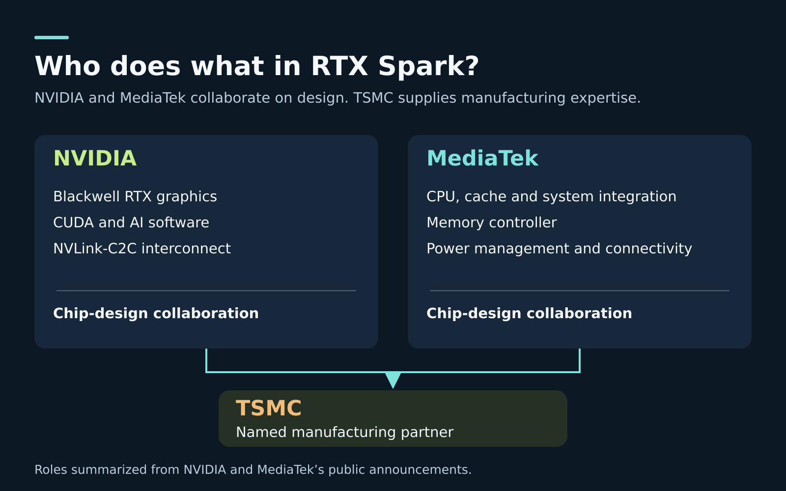
NVIDIA and MediaTek co-developed the technology behind RTX Spark, and MediaTek identifies TSMC as its manufacturing partner for the project. NVIDIA brings the RTX graphics and AI platform. MediaTek contributes CPU, memory, power and connectivity engineering. TSMC brings the chip-manufacturing side. Together, that work puts an Arm CPU, Blackwell graphics and shared memory inside the laptops carrying the N1X name.
How those parts work together drives the buying decision. A large local AI project needs usable memory as well as GPU power. An editing setup needs compatible applications, plug-ins and peripherals. Understanding the chip’s design helps you read a laptop’s specifications and ask the right questions before spending your money.
NVIDIA supplies the RTX and AI foundation
NVIDIA’s May 31, 2026 announcement describes RTX Spark as a combination of Blackwell RTX graphics, a Grace CPU and the company’s NVLink-C2C connection between them. It also explicitly credits MediaTek’s collaboration on the custom CPU design.
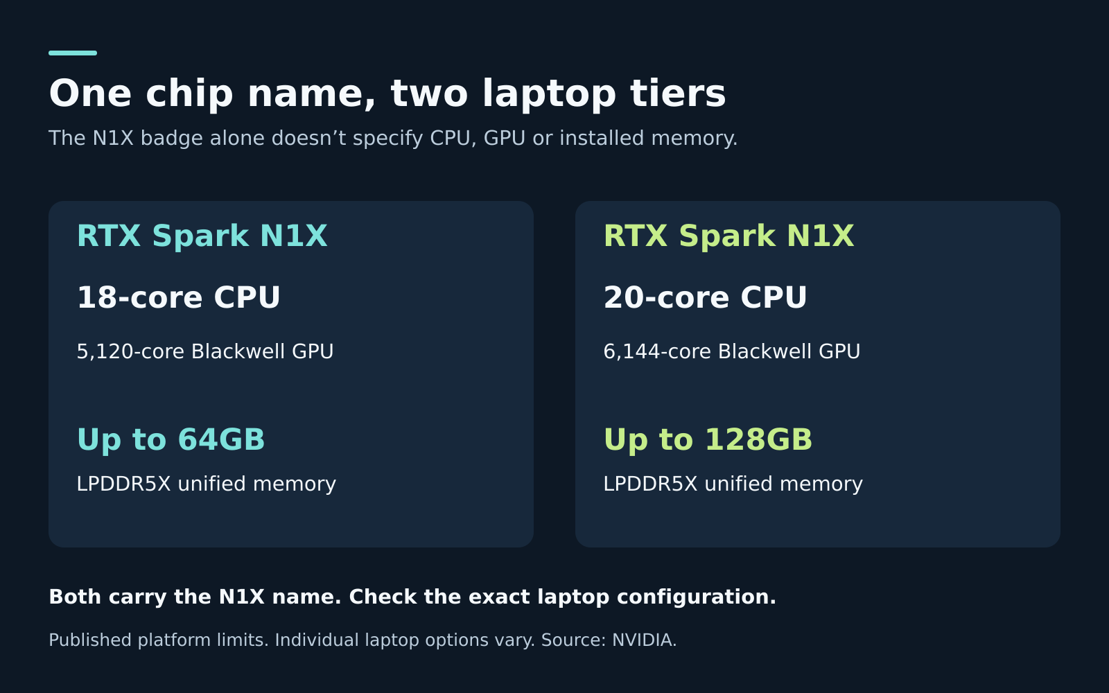
That’s the platform name. N1X identifies the processors listed in NVIDIA’s laptop specifications. Both laptop tiers carry that name: one has an 18-core CPU and 5,120-core GPU, while the higher tier has a 20-core CPU and 6,144-core GPU. Their supported memory ceilings are 64GB and 128GB, respectively. The exact configuration deserves a close look even when two laptops have the same N1X label.
NVIDIA’s contribution also includes CUDA, its GPU-computing platform, and the RTX tools used by creative applications and games. If your work already depends on CUDA, that software connection is a practical reason to consider the platform. You can evaluate the machine around the tools you use for rendering or local AI, then check their Windows-on-Arm support.
MediaTek helped engineer the whole system
MediaTek’s June 1 announcement describes a substantial engineering role: CPU and cache technology, system integration, a proprietary memory controller, power management and connectivity. Its memory controller supports configurations with up to 128GB of unified memory.
These are central parts of a laptop processor. The CPU handles general-purpose work, the memory controller moves data to and from memory, and power management governs how the hardware uses its available electrical power. Bringing those pieces together is what lets a machine run a demanding application and still fit in a bag.
There’s a useful detail behind the Grace CPU name. NVIDIA’s technical guide identifies Arm Cortex-X925 and Cortex-A725 CPU cores inside the chip. Ten of each go in the 20-core version; the 18-core version uses nine of each. Those cores sit inside a custom system with the surrounding cache, memory and other subsystems.
MediaTek’s contribution reaches into the design decisions that let the CPU, GPU and the rest of the platform operate as one system.
TSMC provides the manufacturing expertise
MediaTek names its manufacturing partnership with TSMC in its account of the integration. TSMC’s role belongs on the fabrication side of the story: the company’s foundry business manufactures chips designed by its customers.
Chip design specifies what the circuits do and how they’re organized. Fabrication turns that design into physical silicon through a manufacturing process. Both require deep engineering expertise, but they answer different parts of “who makes the chip?” NVIDIA and MediaTek describe the product and system-design collaboration; TSMC is the manufacturing partner named in that account.
A foundry name alone tells a buyer little about battery life or sustained speed. Those results also depend on the chip design, power limits, cooling and the finished laptop. Judge those qualities through testing of the exact machine you’re considering.
Arm and unified memory describe different things
Arm describes the CPU architecture, including the instructions software uses to make the processor do work. Arm distinguishes that architecture from the particular design that implements it. Unified memory architecture, or UMA, describes how the CPU and GPU access physical memory. They’re separate design choices. NVIDIA’s own programming guide cautions developers against assuming unified memory is exclusive to Arm systems.
On this platform, the CPU and integrated GPU share physical DRAM. That gives graphics and AI software a different memory arrangement from a conventional discrete-GPU laptop, where the graphics processor has its own VRAM. For a large local model or 3D project, access to a substantial shared pool is a meaningful capability to investigate.
Installed memory still needs context. NVIDIA divides the platform’s memory into three regions: a GPU-only reservation, a CPU/GPU shared region and a CPU-only region. A laptop advertised with 128GB therefore has less than 128GB available for GPU allocations. Windows and other applications need room too.
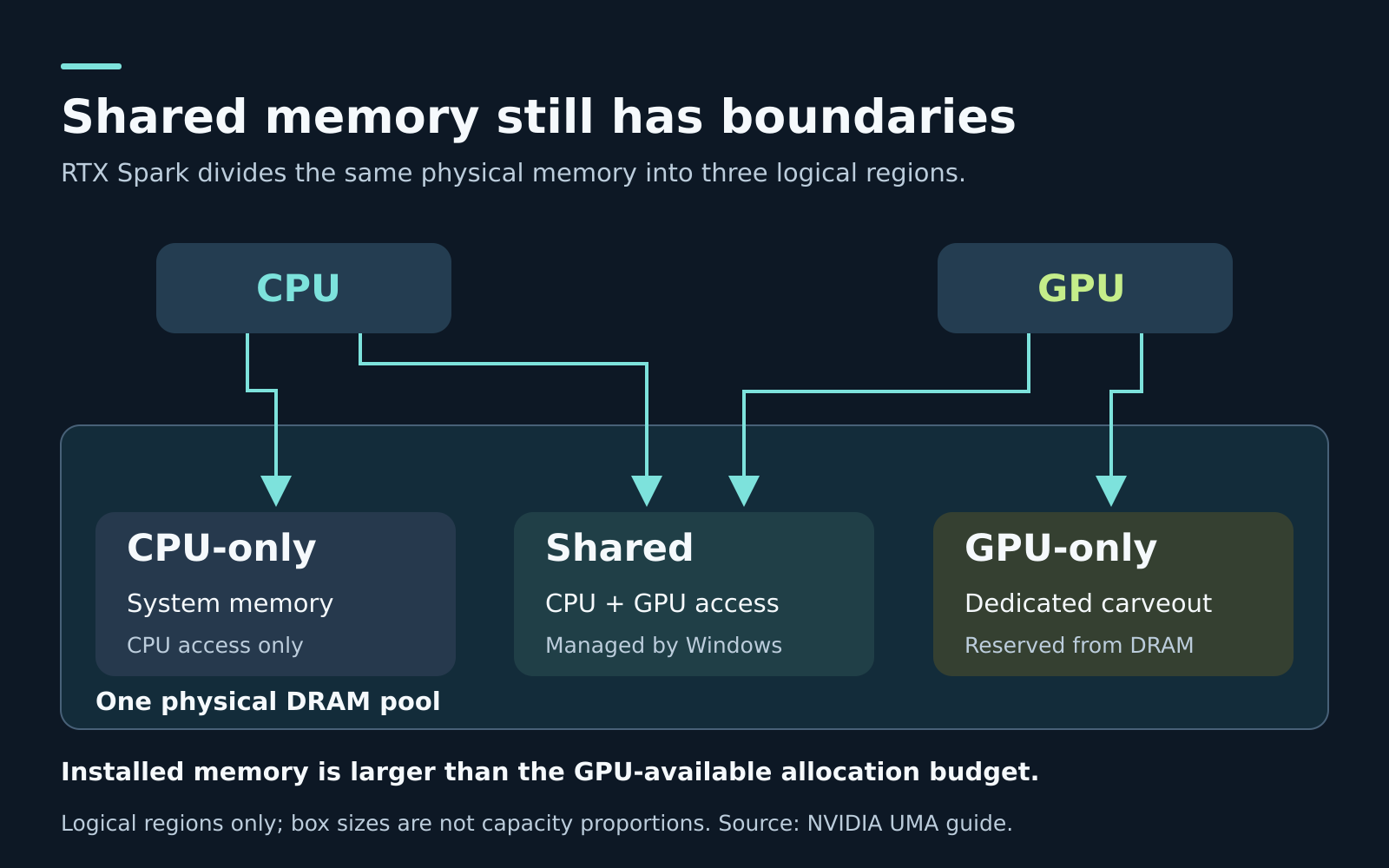
Software also has to use that arrangement well. NVIDIA documents shared buffers that the GPU can access without an explicit CPU-to-GPU copy, alongside GPU-focused allocations for data such as model weights. That’s a concrete mechanism through which integration can help. It doesn’t establish an automatic speed advantage for every application or turn a memory-capacity number into an AI benchmark.
Buy the configuration that fits your work
Start with the applications, plug-ins and peripherals you rely on. These laptops run Windows on Arm, and NVIDIA documents native Arm64, Arm64EC and emulated application paths. Microsoft’s compatibility guidance also makes the driver requirement clear: connected hardware needs a compatible driver built into Windows or supplied by its manufacturer. An audio interface, specialist scanner or other essential accessory belongs on your checklist alongside the main application.
Then match memory to the work you’ll actually put on the laptop. A local-AI developer should check the intended model, software backend and working memory requirement. A video editor should check the footage, effects and plug-ins in a real project. Buying the largest memory option only makes sense when the extra capacity solves a problem you have.
Finally, compare the finished laptops. Screen quality, keyboard, ports, cooling, battery endurance and service support remain part of the purchase. Shared chip technology gives manufacturers a common foundation; you’ll live with the choices each one builds around it.
Three companies built this platform together: NVIDIA’s graphics and AI software, MediaTek’s system engineering and TSMC’s manufacturing expertise in a Windows laptop platform. Put that combination to work by checking your software first, choosing the right N1X and memory configuration, and looking for measured results from the actual laptop on your shortlist.